
- Details
-
Features and characteristics
▎Flexible packaging and mounting machine for chip to wafer TCB process
▎Can be switched in a short time to correspond to the TCB process of chip to substrate
▎Can be used with Face down process (Face up process is optional)
▎Can correspond to TCB (NCP/NCF/TC-CUF), C2, C4, FO-WLP and other processes
▎High -precision patching is achieved through Shinkawa INVS (Non vibration system) technology
▎Through FFG (Force Free Gantry), it can handle high loads up to 350N
▎Using high-speed pulse temperature control system, heating/cooling can be performed in a short time to achieve high output
▎Can handle various suction methods and can transport thin chips
▎The product variety automatic switching function allows the chip mounting function of 4 different chips, which can correspond to 2.5D and 3D stacking.
▎High output/miniaturization through Multi Head function
Application Scenario
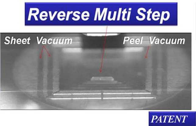
For connection, gripping thin objects, Pulse Vacuum Reverse Multi Step (PV-RMS)
NAND flash memory, which is developing towards multi-layering, is cut to 30um thick, even with the adhesive layer. It is so thin that it is easy to bend and break. In order to bond components, the technology of grasping the chip is essential, but it is extremely difficult to handle extremely thin chips at the same time. The grasping method that cleverly utilizes the bending characteristics of components is Pulse Vacuum Reverse Multi Step (PV-RMS). By intermittently vacuuming from the outside of the sheet, the recovery force of the bent chip is utilized to promote efficient chip peeling. It is not only effective for thin chips, but also for chips with fragile Through Silicon Via (TSV) structures, and it can be said to be a key technology in the future field of electronic component bonding.

Efficient connection, multi-segment chip one-time patching
As chips become thinner, denser, and larger, high demands are placed on the bending and assembly accuracy during flip-chip assembly. As a solution, we proposed the Thermal Compression Bonding (TCB) process, which is suitable for the most advanced storage (HBM, HMC, etc.) using TSV (Through Silicon Via). This process is to perform tin-lead alloy bonding of the electrode terminal and curing of the Underflow while applying pressure and heating. Since this process requires about 10 seconds per piece, it limits the improvement of productivity.
Shinkawa has conducted basic research and development on various core technologies that may be suitable for bonding multiple chips together (Gang bonding, Collective bonding, etc.). Through the establishment of various core technologies and the use of the high-speed TCB Bonder FPB series, the research results that can increase productivity by about 20 times were announced at ECTC2017.